
If you read my blog post on NAND gates or viewed my NAND or NOR video all the way to the end, you’ll recognize this circuit. It is a 16 instruction microprocessor I designed for a homework assignment in a class I took years ago. When I found the program Logisim, I figured it would be nice to put this CPU in it and see if the design works. This blog post is also useful to anyone who wonders “What can you do with ANDs, ORs, NANDs, and NORs anyway?” or anyone who wants to know how to simulate digital logic circuits.
Since Logisim is a JAVA program, you’ll need at least Java version 5 (also known as 1.5) to run it. It’s also known as Java Runtime Environment or JRE. You can download Logisim and JAVA for free from the addresses at the end of this post. Don’t be overwhelmed by all the links – I provided as many different links as possible since over time websites change and go away.
It’s important to discuss an attribute of some of Logisim’s components that could become an issue in your design. Some components are triggered by a pulse on an edge that might not be as expected. As expected, triggering can occur on a high-level, or a low-level. But it can also occur on the rising (or positive) edge or the falling (or negative) edge. And some components can only be triggered on a rising or falling edge. Later on you’ll see how this can cause problems.

So here’s my processor design in Logisim. BTW, if I remember correctly, the teacher never collected or graded the homework, so there was no absolute way of knowing if my design was correct. Also, for the assignment, we didn’t have to determine things like edge triggering, whether it’s rising or falling, etc. So there was a little bit of adjusting required to get the CPU to work in Logisim. BTW, the original design was a 20-bit processor, but to make things easier, I made it an 8-bit processor in Logisim. It would be rather trivial to make it 20 bit as designed.
I’ll highlight some of the components of my CPU design. You should be able to click or right click on the images for bigger versions.


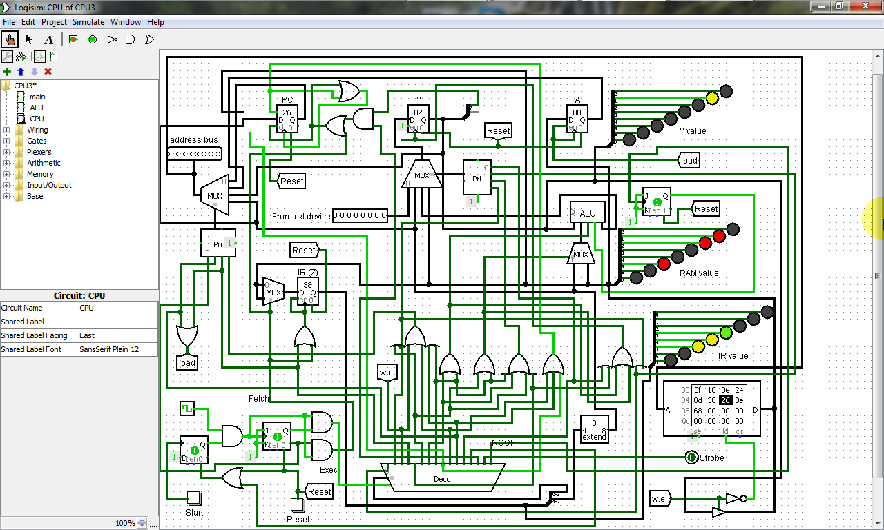
These flip-flops create a resetable and haltable fetch-execute cycle.


D flip-flops. This one functions as the CPU’s instruction register or IR for short. The instruction register also contains the Z register which can be thought of as a virtual register since it is really part of the instruction and not a separate register.
8. We need a splitter as well. It splits a multi-bit value into desired pieces or combines pieces into a desired multi-bit value. This one separates the opcode from the Z register. The other splitter (8b) grabs the most significant bit of the Y register to signal a negative number in the Y register (assuming the value is a signed value).
9. This is a controlled buffer. It’s also known as a tri-state buffer or a tri-state gate. It outputs the input if the control line is 1. This is used to allow the RAM’s data line to be for both reading and writing.
10. Finally, to make the circuit nicer looking, tunnels are used. A tunnel represents a wire connecting all tunnels of the same name together.
Later, we’ll need a bit extender, which extends the bit width of the input.


Internally, a CPU moves data between the different parts of the machine. RAM to registers, registers to RAM, RAM to ALU, ALU to register, etc.

This is the instruction set this CPU executes. LOADI transfers the Z register to the Y register. LOAD transfers the memory contents pointed to by the Z register to the Y register. JUMP changes the program counter to the specified location. DATA IN transfers data from a hypothetical external device to the Y register. STROBE sends a pulse to the external device (presumably to tell it to send data). NOOP doesn’t do anything. You can most likely figure out the rest.
The instructions are orchestrated by the decoder with each line representing one of the instructions from LOADI to NOOP. Here’s the various things that are done to execute each instruction. BTW, the port numbers refer to the numbers written next to the encoders, etc. on my homework solution shown at the beginning of this post. Notice on opcode 3 and 10 (which are STORE and JUMP II) there’s an asterisk that indicates that step isn’t implemented. This is because I don’t know of any good way to select two different encoder ports on the same encoder at the same time. I thought maybe you could use two encoders and have a controlled buffer or mux select which address line goes to the address bus during different parts of the pulse, but that seems too complicated and kludgy. So for now those instructions aren’t fully implemented.


Refer to this animated GIF for proof this original CPU design does at least somewhat work (and especially refer to the video at the end of this post for a much better video covering all of this). In the animated GIF, you’ll see loading of a few instructions and running them. The instructions will do a few STROBEs, NOOPs, a transfer from external device to the Y register, and a HALT. You can see the activated lines in bright green. A CPU works by doing a Fetch-Execute cycle. First fetching an instruction from RAM, putting it in the instruction register. And then executing it. The flip-flops make sure the fetch-execute cycle occurs continuously as long as the CPU is in a running state.
This design does have a few problems though, so let’s fix the problems and while we’re at it, improve the design some. The first problem is that for opcode 5 and 7 which add and subtract using a value in memory, there was no path to send the Z register value to the address bus. This was solved by adding two lines to the OR labeled A. Another problem was that there was no pre-fetch line. B solves that.

As for improvements, I added some LEDs to visually show the contents of the Y register, the instruction register, and the RAM data line. I also put in a bit extender that I mentioned earlier. It’s there because the registers require an 8-bit value, but the part of the instruction that is the Z register is only 4 bits. So the 4 most significant bits of the instruction are combined with the 4 new most significant bits (which are set to 0 in this extender) to form the contents of the essentially virtual Z register. This arrangement guarantees that only the Z register part of the instruction is sent to the other parts of the processor that require the Z register. There’s also some triggering circuitry added to the program counter because of what I consider the kind of odd way Logisim’s counter is controlled. I also added Reset lines to each register (see CPU image below) so that the contents are cleared when Reset is hit. It’s not necessary, but it’s a good idea.


Addendum: I fixed this problem in my "My CPU: Goodbye Gated Clocks! Hello Indirect Jumps (Now With More Programs)" video. Look for it (and my Floating Point version of this CPU if you would like) at: https://youtube.com/mrmcsoftware/videos or view all my Logisim CPU videos using my playlist: https://www.youtube.com/playlist?list=PLLQoKy-hD9LDG8PeMiZYN15O2eP1DfYTB


This will create a KITT effect from the Knight Rider TV show. Or, if you prefer a Cylon effect….. Unfortunately, there’s no instruction to determine if a value is 1 (or any specified number for that matter), so we can’t reverse the direction back. Thus the effect ends. Program 2 creates an effect that is fully repeatable.
Well, as you can see, the CPU isn’t perfect but it does run. As I stated in my NAND blog post and NAND and NOR videos, it would have been nice to create this CPU as an integrated circuit in my University’s integrated circuit manufacturing lab. With Logisim, the design could be tested before committing it to silicon saving a lot of trouble.
In Logisim, components such as counters, MUXes. etc. aren’t built up by building upon basic logic gates. They are simulated by software procedures or classes. In order to show what these components consist of, I had to build them myself in Logisim. By doing this, I figured out some statistics. If the original CPU design with corrections and 8-bit rather than 20-bit data width was built, it would require 348 NANDs, 341 ANDs, 8 NORs, 130 ORs, and 164 NOTs. If this was implemented using a CMOS design, it would require 2,289 PMOS and 2,289 NMOS transistors for a total of 4,578 transistors. The 20-bit CPU would require at least 10,458 transistors. I’m closing in on you Pentium. Well, not really at all.
Give Logisim a try. Maybe you can use it to come up with an even better CPU.
Here’s my video covering all of this in a much better way:
NEW: Here's my new video showing my even more improved CPU in a full-fledged computer (via Logisim):
Here are links to various Logisim versions and Java:
http://www.cburch.com/logisim/ (project website)
https://sourceforge.net/projects/circuit/ (download page)
https://sourceforge.net/projects/circuit/files/latest/download (easiest download link)
Since the original creator of Logisim has discontinued work on it due to time constraints, others have created other versions using his code. Here are some different “forks” of Logisim:
http://reds-data.heig-vd.ch/logisim-evolution/logisim-evolution.jar (compiled program direct link. Need to “java -jar logisim-evolution.jar”)
https://github.com/reds-heig/logisim-evolution (source code (needs to be compiled) – click “Clone or download”)
https://codeload.github.com/reds-heig/logisim-evolution/zip/master (source code direct link)
https://github.com/lawrancej/logisim (needs to be compiled. Click “Clone or download”)
https://code.google.com/p/logisim-iitd (project page)
http://www.cs.cornell.edu/courses/cs3410/2017sp/logisim/logisim-evolution.jar (download link)
http://www.cs.cornell.edu/courses/cs3410/2017sp/ (course page)
Also, Digital is a similar program:
https://github.com/hneemann/Digital (project page and download section. Needs to be compiled. Click “Clone or download”)
https://github.com/hneemann/Digital/releases/download/v0.9/Digital.zip (compiled program direct link)
If you need JAVA:
http://www.oracle.com/technetwork/java/javase/downloads/jre8-downloads-2133155.html
http://www.oracle.com/technetwork/java/javase/downloads/index.html (general download page)
https://www.java.com (general java page)
Whichever Java package you choose, for safety reasons, you might want to disable the JAVA browser plugin if it gets installed (not to be confused with Javascript).
No comments:
Post a Comment