 |
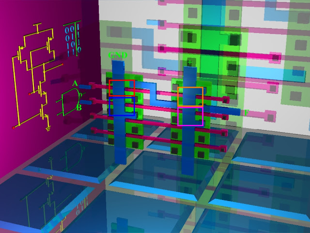
| A raytraced colored glass integrated circuit mask layout of a NAND logic circuit made from a gate array. |
Since my raytraced NAND circuit image
(Integrated Circuit Mask Layout, etc.) is the most popular (in terms of
views and downloads) image in my deviantArt gallery, I decided to write a
blog post explaining the electronics behind this circuit.
Admittedly, chances are anyone interested in this image already knows
the electronics part, but in case they don’t… Now for the
disclaimer: I modeled (for my raytracer) the IC mask layout about
11 years ago, and I had a class in this subject about 26 years ago, so
it’s not exactly fresh in my mind.
 |
| My Original Raytraced NAND IC Mask Layout (Modeled 11 Years Ago) |
 |
| Annotated NAND Schematic (Encased In Glass) |
 |
| Annotated NAND IC Mask Layout |
The two images with annotations show how
the schematic matches the IC mask layout. For this discussion,
GND is ground, + is Vdd, F is the NAND gate output, A and B are the NAND
gate inputs, and the colored rectangles surround the individual
transistors (which are color coded to match).
I’ll start by describing the schematic of the CMOS NAND logic circuit. The two top transistors (side by side) are PMOS (p-channel metal-oxide-semiconductor) which are normally on (meaning when the voltage on the transistor input (gate) is zero, current flows between the drain and the source). So, as long as either A or B or both are off (0), the output F receives Vdd (presumably, 5 volts). The two bottom transistors are NMOS (n-channel metal-oxide-semiconductors) which are normally off (meaning when the voltage on the transistor input is zero, current doesn’t flow between the drain and the source). In this configuration, both A and B have to be on (5 volts) in order for F to be tied to ground (thus a 0), and in this case, the top two transistors would be off (thus not providing Vdd). Since both NMOS and PMOS transistors are used, this circuit is considered CMOS (complementary metal-oxide-semiconductor). By the way, the direction of the arrows (of the transistors) in the schematic show which type of transistor it is, and the legs with the arrows are the sources (as opposed to the drains).
Now, I’ll describe the Integrated Circuit (IC) mask layout. Integrated circuits are created using a sequence of masks. The basic mask sequence is transistor area mask, polysilicon gate definition mask, contact area mask, and then metal definition mask. Thus a mask layout represents the masks that would be used (the actual masks would have to be checked and modified to adhere to various spacing requirements). The blue areas are metal. The gray areas are cuts which create possible contacts (for the metal areas). The red areas are polysilicon (gates). The green areas are heavily doped n+ or p+ regions (diffusion) (sources and drains). Technically, the NMOS transistors (the green area on the left), have an “understood” or “assumed” p-type well diffusion. I didn’t model that (p-type well diffusion) distinction. Anywhere the red overlaps the green (polysilicon overlaps diffusion), a transistor is formed. The red lines conduct electricity from end to end. The left block creates the two bottom transistors (in the schematic), and the right block creates the two top transistors. Therefore, the left metal strip is ground, and the right metal strip is Vdd (+5v). The two red lines with metal attached are the NAND gate inputs (A and B). The metal on the far right (attached to the green area through a cut) is the output of the NAND gate. The squiggly metal in the middle connects the two sets of transistors together and to the output of the NAND gate. With this information, you should be able to see how the mask layout matches the schematic.
Blank gate arrays are formed on the silicon wafer (with the polysilicon, diffusion, cuts, and basic metal strips (not contacting anything) all formed) in the first stages of the process. Then all a manufacturer has to do is make the metal connections needed to form the desired circuit. Kind of like writing to a blank CD-R (not as easy though). Each chip (gate array) may have several thousands of transistors (many more blocks than what I modeled). The modern incarnation of gate arrays is FPGA (Field-Programmable Gate Array). These are fully manufactured blank so to speak, and are configured (or programmed) by the customer – no manufacturing required. They even can be re-programmed. These really are like writing to a blank CD-RW and as easy (as long as you know the coding language).
 |
| My Raytraced NMOS Inverter IC Mask Layout |
 |
| My Raytraced NMOS Inverter IC Mask Layout (Modified) |
By the way, I modeled another IC mask
layout – an NMOS inverter. I won’t bother describing that one,
except to say the yellow area is a depletion implant, and the four metal
lines at the bottom are inverter input, ground, inverter output, and
Vdd respectively. Also, in case it wasn’t obvious, in the NAND
scene, the white back wall has many colored shadows/projections of the
glass NAND mask layout because there’s more than one light – the lights
are in different locations. The effect is easier to see in my
“Project GlassWorks…” video on my YouTube channel.
It’s too bad (for me) my university
built an integrated circuit fabrication lab after I graduated (B.S. in
Computer Engineering) – maybe I could have made some of these
circuits. Also, too bad they created a supercomputer after I
graduated. But the professor responsible for creating it was on my
thesis committee when I pursued my Masters (in Computer Science), so I
did get to see it during its construction.
On another subject, I did design a simple 16 instruction microprocessor for a homework assignment. Maybe it could be made using a gate array. Of course, each one of those boxes contains many logic gates, so it’s really more than it appears.
 |
| 16 Instruction Microprocessor I Designed |
I created a YouTube video showing all of this and some more stuff:
Also, I created a video showing the CMOS
circuits for NAND, AND, NOR, and OR as well as the SPICE analysis of
these circuits using various SPICE tools for Windows/Mac and
UNIX/Linux. This video shows you how to use these tools to simulate the
circuits.
And, I created a video showing the testing, simulation, and improvement of my above mentioned microprocessor. Logisim is used to do this. This video also shows various digital logic basics, such as multiplexers, decoders, flip flops. etc.
No comments:
Post a Comment